PSPI
PSPI (photosensitive polyimide) is a very important semiconductor material, and also a very bottleneck material.
What is PSPI?
PSPI, the full name of which is “photosensitive polyimide”, combines the excellent physical and chemical properties of polyimide (PI) with the characteristics of photosensitive materials. PSPI is similar to photoresist. Under the radiation of ultraviolet light, α rays, X-rays, etc., the structure of the irradiated part will change, and it can be dissolved in the corresponding solvent, and can be used to make precise patterns.
What are the excellent properties of PI?
- Good dielectric properties: The dielectric constant is usually between 3.0 and 3.5, and can be reduced to 2.5 after improvement; the dielectric strength is very high, usually between 200 and 300 kV/mm; the volume resistivity is very high, between 10^16 and 10^18 Ω·cm; the surface resistivity is also very high, usually in the range of 10^13 to 10^16 Ω. PI has excellent electrical insulation at high voltage and different frequencies, and can effectively prevent current leakage and electrical breakdown.
- Wide operating temperature range: maintains its physical properties at extreme temperatures (between -269°C and +400°C)
- Very low thermal expansion coefficient: The thermal expansion coefficient is about 20 to 50 ppm/°C. That is, the volume changes very little when the temperature changes.
- Excellent mechanical properties: high strength; high toughness; strong impact resistance;
- Good chemical stability: resistant to many organic solvents, acids, alkalis, etc.
What are the advantages of PSPI over non-photosensitive PI?
Greatly simplifies the processing steps and saves costs.
PSPI process steps
Coating – soft baking – exposure – development – curing
PI process steps
PI coating – curing – photoresist coating – photoresist soft baking – photoresist exposure – photoresist development – photoresist post-baking – PI etching – photoresist removal
PSPI structure?
- Main chain: The main chain is composed of repeated imide ring structures (-CO-NH-CO-).
- Photosensitive groups: Photosensitive groups are functional groups that can undergo chemical reactions under the irradiation of light of a specific wavelength. The introduction of photosensitive groups enables the material to crosslink or decompose under light. Common PSPI photosensitive groups include: epoxy groups, double bonds, azo compounds, etc.
- Other functional groups: Other special functional groups are introduced to improve its electrical properties or processability.
Application of PSPI in the semiconductor industry?
Semiconductor manufacturing:
- PSPI can be used as an insulating layer and a dielectric layer to prevent electrical crosstalk between different layers in the chip; it can also be used as a protective layer, such as in processes such as etching or ion implantation, PSPI can protect the wafer surface from damage.
- Wafer-level packaging: PSPI is mainly used as an insulating layer, a protective layer, and a carrier for electroplating circuits.
- PCB board manufacturing: It is usually used as a barrier layer for the Cu board, and then the Cu board is etched with a solution; then the PSPI dielectric layer is laminated with the Cu board.
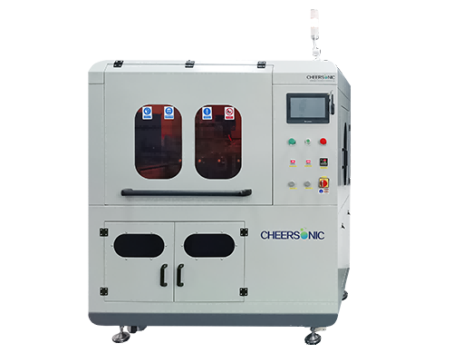
Ultrasonic spraying systems have been proven to be used in various applications that require uniform and repeatable photoresist or polyimide film coatings. The thickness control range is from submicron to more than 100 microns, and any shape or size can be coated.
Ultrasonic spraying technology is used for semiconductor photoresist coating. Compared with traditional coating processes such as spin coating and dip coating, it has the advantages of high uniformity, good encapsulation of microstructures, and controllable coating area. In the past 10 years, it has been fully demonstrated that the 3D microstructure surface photoresist coating using ultrasonic spraying technology, the prepared photoresist coating is significantly higher than the traditional spin coating in terms of microstructure wrapping and uniformity Craft.
The ultrasonic spraying system can precisely control the flow rate, coating speed and deposition volume. Low-speed spray shaping defines atomized spray as a precise and controllable pattern to avoid excessive spray when producing a very thin and uniform layer. The ultrasonic spray system can control the thickness from sub-micron to more than 100 microns, and can coat any shape or size.
About Cheersonic
Cheersonic is the leading developer and manufacturer of ultrasonic coating systems for applying precise, thin film coatings to protect, strengthen or smooth surfaces on parts and components for the microelectronics/electronics, alternative energy, medical and industrial markets, including specialized glass applications in construction and automotive.
Our coating solutions are environmentally-friendly, efficient and highly reliable, and enable dramatic reductions in overspray, savings in raw material, water and energy usage and provide improved process repeatability, transfer efficiency, high uniformity and reduced emissions.
Chinese Website: Cheersonic Provides Professional Coating Solutions

