Photolithography Process Overview
Photolithography Process Overview – Photoresist Coatings – Cheersonic
Photolithography is the art and science of producing patterns on a substrate. Today, the term is most commonly used in semiconductor processing. Other adjectives are often used to more specifically define the technology, such as optical lithography or photolithography (using ultraviolet light to produce patterns), imprint lithography (pressing or stamping a mold into a material to produce patterns), electron beam lithography (using an electron beam to produce patterns), or EUV lithography. The most common form of lithography used in high-volume manufacturing is optical lithography.
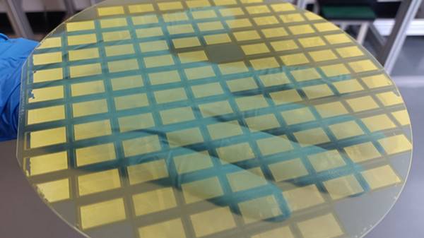
A highly simplified description of the process is as follows. A substrate (usually a silicon wafer) is typically coated with a thin film or stack of multiple layers of a functional material that can serve a variety of purposes, such as a low-k or high-k dielectric, an etch-resistant hard mask, or a conductive layer. A photoresist is a light-sensitive material, usually composed primarily of organic polymers, which is then spin-coated onto the thin film stack. The term photoresist is often shortened to photoresist, which is also a more general term for this class of materials; especially because many alternative and future exposure sources for photoresists are not exposed to photons, but rather to electrons, ions, or other patterning physics sources.
UV light is then shined onto a mask that selectively allows light to pass through certain areas to create a pattern in the photoresist. Masks were historically made of quartz with a chrome pattern on top that controlled where the light passed through the mask. The pattern of UV radiation causes chemical changes in the photoresist that selectively change the solubility of the exposed areas in a liquid called a developer. The wafer is typically baked after the exposure step [called a post-exposure bake (PEB)] to further induce chemical changes in the exposed areas.
Next comes the development step, where the developer is poured or sprayed onto the photoresist, causing certain areas of the photoresist to dissolve while other areas remain on the wafer. The exposed areas will either dissolve or remain depending on the hue of the photoresist. Positive photoresists are those whose exposed areas dissolve during the development process; the solubility change is usually due to a chemical reaction that occurs during the exposure process or in the PEB that changes the polarity or functional groups of the photoresist. Negative photoresists are those whose exposed areas do not dissolve during the development process; the exposed areas do dissolve. Changes in the solubility of these materials can likewise occur through a number of different methods, but the two most common are cross-linking to form a high molecular weight network structure and changes in the functional groups of the photoresist, which affect polarity.
Finally, an etching process is used to transfer the remaining pattern in the developed photoresist to the underlying film stack. This etching process can be either wet or chemical etching, where liquid chemicals selectively remove the underlayer (UL) while having minimal effect on the remaining photoresist. However, it is more common to use plasma etching for etching, where energetic particles selectively etch the UL and not the remaining photoresist. Plasma etching can achieve a high level of control and selectivity at both nanoscale and wafer-size scales by varying various parameters in the etching chamber, such as etching gas and species, voltage, bias on the wafer, pressure, and local wafer temperature. Plasma etching can be varied from an isotropic to a highly anisotropic etch profile by controlling the timing and type of gases used. Recent advances have even shown the possibility of atomic-level control with the introduction of atomic layer etching.
After all desired modifications have been made in the underlying film stack, any remaining photoresist is removed by a plasma or chemical stripping process. This lithography process is then repeated (sometimes multiple times) for each layer of the device to create a complete integrated circuit.
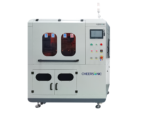
Ultrasonic spraying systems have been proven to be used in various applications that require uniform and repeatable photoresist or polyimide film coatings. The thickness control range is from submicron to more than 100 microns, and any shape or size can be coated.
Ultrasonic spraying technology is used for semiconductor photoresist coating. Compared with traditional coating processes such as spin coating and dip coating, it has the advantages of high uniformity, good encapsulation of microstructures, and controllable coating area. In the past 10 years, it has been fully demonstrated that the 3D microstructure surface photoresist coating using ultrasonic spraying technology, the prepared photoresist coating is significantly higher than the traditional spin coating in terms of microstructure wrapping and uniformity Craft.
The ultrasonic spraying system can precisely control the flow rate, coating speed and deposition volume. Low-speed spray shaping defines atomized spray as a precise and controllable pattern to avoid excessive spray when producing a very thin and uniform layer. The ultrasonic spray system can control the thickness from sub-micron to more than 100 microns, and can coat any shape or size.
About Cheersonic
Cheersonic is the leading developer and manufacturer of ultrasonic coating systems for applying precise, thin film coatings to protect, strengthen or smooth surfaces on parts and components for the microelectronics/electronics, alternative energy, medical and industrial markets, including specialized glass applications in construction and automotive.
Our coating solutions are environmentally-friendly, efficient and highly reliable, and enable dramatic reductions in overspray, savings in raw material, water and energy usage and provide improved process repeatability, transfer efficiency, high uniformity and reduced emissions.
Chinese Website: Cheersonic Provides Professional Coating Solutions


