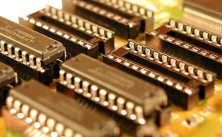
Medical grade PCB board circuit board design
Medical grade PCB board circuit board design – Cheersonic ultrasonic nozzle
Medical-grade PCB boards are the key to unlocking the future of health and care. As the healthcare industry moves towards more advanced technology and more sophisticated automation levels, medical robots with advanced capabilities will become the norm.
They will not only handle basic maintenance tasks. Communication and interaction with robotic staff, nurses, and even makeshift surgeons may soon be seen in consulting rooms or hospitals. This scenario is a little weird, but given that most of these technologies are very reliable, it is entirely possible to use them to do things that human experts cannot.
The design process may vary slightly, but the overall architecture is basically the same. The following are some of the general steps in the design and development phase of the medical robot PCB board:
1. Create a schematic. The first step is to gather all the relevant information and start creating a PCB drawing or schematic. This is the initial planning stage, and careful consideration should be given to the board type for the design, material selection, power consumption requirements, and other key factors such as sequencing or splitting the internal electrical layers. Medical grade PCB boards have to follow very complex technical specifications.
It is important to understand that the schematic is only a general guideline. While specification requirements must be met, some other elements may change as work = progresses. For example, if certain designs are found to be inappropriate or not as efficient as expected, a different device layout design may be considered.
2. Select the board enclosure. The casing is important to protect the circuit board from being exposed and protected from other conditions – this is especially important for the equipment inside the robot. However, since the PCB board is usually a custom design, it is also necessary to customize the housing to ensure that it matches the circuit board. Significant time is invested in selecting materials and designs, and sourcing or producing components before development begins.
Here are some things to consider when choosing an enclosure:
•Which configuration is best for the enclosure – vertical or horizontal?
• How many layers does the enclosure need to support?
• Does the board need to be cut or trimmed to fit the enclosure shape?
• Where can holes be drilled and what safety precautions are in place?
• What is the ideal trace width and spacing?
• Are there electrical clearances and inspection holes, and do they need to be specially added?
• How long does it take to produce or acquire additional components?
3. Device placement. Device placement takes the longest time, both in the design and assembly stages. The device layout must meet the mechanical and electrical requirements, but there are also performance aspects to consider—circuits must fit together. This may require moving the device around the board and testing the response or response time to determine the best configuration.
Also, in addition to the preferred device, alternative devices should be stocked. It is important to test its success and failure rates. If a device is found to be non-compliant, a replacement can be used—provided the replacement has been tested.
4. Plan the main current direction. While there are some automatic routing tools, their limitations need to be recognized. Such tools do not always follow the optimal flow, so it is necessary to check the power consumption curve and make manual adjustments if necessary.
Regardless, every PCB design and assembly process should take this into account. Proper spacing, trace width, ground plane, and signal-to-noise ratio (SNR) are key elements in building a PCB.
5. Create test points. Where are the main test points for the board before, during and after assembly? More test points help reduce errors and ensure ideal conditions during operation. What’s more, each board is unique based on the chosen design and layout, so proper testing needs to be evaluated with every change or update—as well as in subsequent product revisions.
Complete documentation is essential, so be sure to document the testing process, location, and results and keep this information safe.
6. Assemble. The final step in the process is, of course, the assembly of the circuit board. This step includes initial board development, solder paste printing and soldering, device picking and placement, and any other minor adjustments. Finally, it must be checked to ensure quality control. Subsequently, through-hole devices are inserted as necessary.
Functional tests must be performed to ensure that the board, all components and the product itself are in good condition.
Article source: Medtec China
Cheersonic is the leading developer and manufacturer of ultrasonic coating systems for applying precise, thin film coatings to protect, strengthen or smooth surfaces on parts and components for the microelectronics/electronics, alternative energy, medical and industrial markets, including specialized glass applications in construction and automotive.