How To Reduce Tape-out Costs?
How To Reduce Tape-out Costs? Spray photoresist onto MEMS wafers – Cheersonic
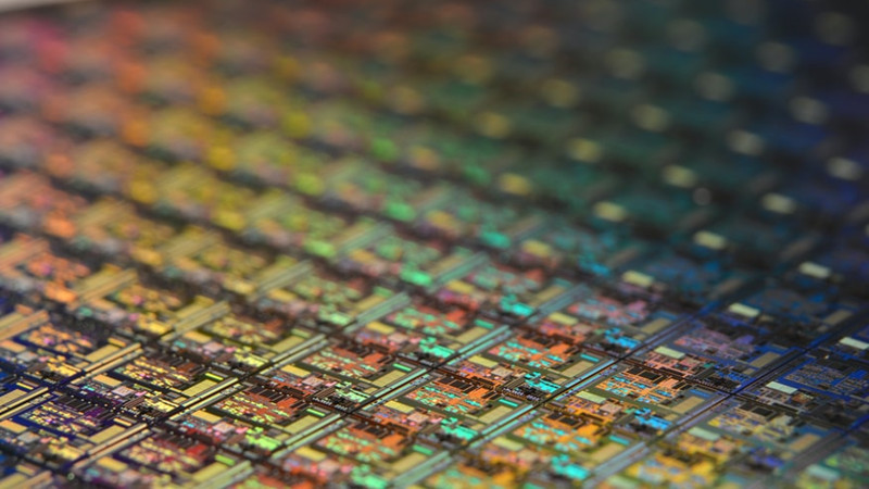
Taping out is expensive, on the one hand, because there are many processes that need to be verified at the beginning, from a circuit diagram to a chip, to check whether each process step is feasible and whether the circuit has the required performance and functions. The chip tape-out process lasts for at least three months (including raw material preparation, lithography, doping, electroplating, packaging and testing), and generally requires more than 1,000 processes. The production cycle is long, so it is also the most important and expensive in chip manufacturing. link.
Under the influence of the above factors, the cost of chip tape-out has become a difficult problem for design companies. So, in the face of the high price of tape-out, is there any way to reduce the cost?
MPW (Multi Project Wafer) is a tape-out method that can help design companies reduce costs. MPW refers to that a wafer is shared by multiple projects. The same manufacturing process can undertake the manufacturing tasks of multiple IC designs, and multiple IC designs using the same process are placed on the same wafer. Dozens of chip samples can be obtained for each design, which is sufficient for experiments and tests in the prototype design stage.
Generally speaking, several companies or institutions buy a set of masks together, and then there will be several chips on the same wafer produced at the same time. After the wafer is cut, the respective chips will be “taken home”. “. The manufacturing cost of this time is shared by all the projects participating in MPW according to the chip area, which greatly reduces the risk of product development.
MPW has a certain process, which is usually organized by a foundry or a third-party service organization. The MPW time point of various processes in a certain year is preset. Usually, the more advanced process, the arrangement The higher the MPW frequency. The foundry will divide the wafer into multiple areas in advance and quote, and each company will book one or more areas according to their own conditions.
This puts a certain schedule pressure on the participants in terms of design and development. But in contrast, the benefits brought by MPW are obvious. The use of multi-project wafers can reduce the production cost of chips, provide designers with practical opportunities, and promote the transformation of chip design results, and the training of IC design talents. The development of small and medium design companies, as well as the development of new products have a considerable role in promoting.
In contrast, the advantage of sharing Mask is to save money, but it may take more time to wait for the time node of the foundry. For those companies that are not short on money or in a hurry, they can of course use a set of Mask (Full-Mask, full mask). All masks in the manufacturing process serve their own designs, usually used to design the finalized volume. production stage. As soon as the machine rings, the gold is ten thousand taels.
However, under the current situation of serious shortage of production capacity, foundries have completely different attitudes towards different customers’ product needs, competitive advantages, market prospects and plans. And the market prospects for the product to make judgments.
In fact, for most small and medium-sized enterprises, in addition to price, they also face many challenges including production capacity and delivery time in the process of tape-out or mass production:
1. Not familiar with the Foundry system, lack of experience in process selection and experience in dealing with Foundry;
2. The entry threshold of mainstream Foundry is high, it is difficult for emerging players to apply for the expected process or support, and the communication cost is high;
3. Lack of systematic supply chain management capabilities, especially in the ramp-up stage of mass production capacity, too optimistic about production capacity, delivery time, and quality;
4. In the case of shortage of production capacity, there is a lack of stocking mechanism, panic placing orders or placing orders again after an order has been placed, resulting in production capacity that cannot keep up with market demand. In addition, changes in delivery dates and fluctuations in production capacity will greatly increase the communication costs between startups and foundries and reduce efficiency.
In this regard, small and medium-sized chip design companies can seek cooperation with a third-party operation service organization with resources, strength and experience to solve the supply chain problems encountered together.
On the other hand, with the self-built professional tape-out FAE team, it not only provides efficient support and management of long-tail customers for cooperative foundries, but also helps small and medium-sized companies to quickly get support for their products, assists customers to choose the best process, and guarantees customers data security.
On the whole, whether in terms of technology, business or production capacity, choosing a reliable third-party organization can assist design companies to solve the current supply chain difficulties and provide optimal solutions.
All in all, companies in these demand tracks are likely to benefit from the business of tape-out service providers.
A chip development project needs to go through a long process from product definition, design, verification and simulation to final tape-out, and as the “ultimate test” tape-out, any small oversight in the previous long process may lead to tape-out failure. Once the film fails, it often means that the company will face losses starting from tens of millions of dollars and miss market opportunities for at least half a year.
For many companies, the failure of tape-out is an unbearable pain.
In this regard, chip design companies, manufacturers, and related industry service platforms and institutions should cooperate closely, complement each other’s advantages, and work together to solve the “tape-out problem” that plagues developers.
Ultrasonic spray has the advantages of precise and controllable spray flow rate, thin and uniform coating, and controllable spray range. It is very suitable for spraying electronic products and is increasingly used for research and production. Ultrasonic spray technology can be used to deposit a uniform coating on substrates of any width. Ultrasonic Spray Electronics technology enables these very thin coatings to be produced with extremely high uniformity, resulting in very accurate and repeatable results to enhance product functionality.