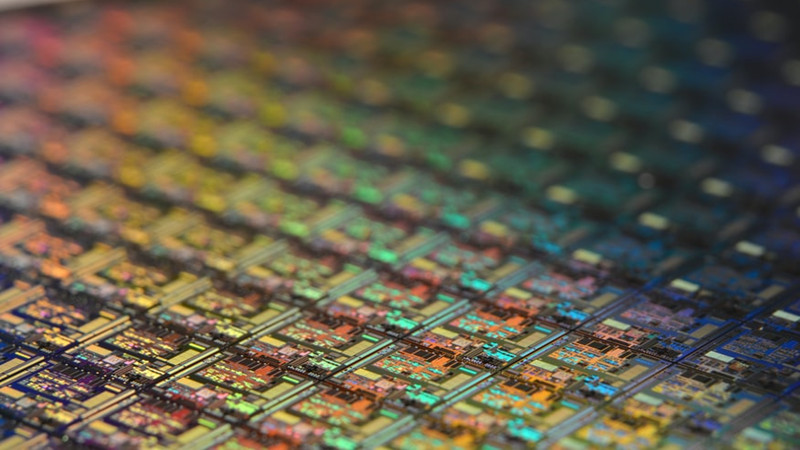
Chip Thin Film Deposition
A chip is a 3D structure formed by stacking a series of active and passive circuit elements, and thin film deposition is one of the core processes in the front-end manufacturing of the chip. From the cross-section of the chip, the chip is composed of layers of nanoscale components. All active circuit components (such as transistors, memory cells, etc.) are concentrated at the bottom of the chip, and the other parts are interconnected by the upper layer of aluminum/copper The formed metal layer and the insulating dielectric layer between the metal layers are composed. The front-end chip manufacturing process includes oxidation diffusion, thin film deposition, glue development, photolithography, ion implantation, etching, cleaning, detection, etc. Thin film deposition is one of the core processes, and its function is to pass physical/chemical on the surface of the wafer. The method is to alternately stack insulating dielectric films such as SiO2 and SiN and metal conductive films such as Al and Cu, etc., on these films, mask pattern transfer (lithography), etching and other processes can be performed, and finally the circuit structure of each layer is formed. Thin-film deposition techniques can be considered an “additive process” in front-end manufacturing, as the manufacturing process requires thin-film deposition techniques to repeatedly stack thin films on the wafer.
Thin film deposition is the key to determining the performance of thin films, and the related process and equipment barriers are high. The key to chip manufacturing lies in the process of transferring the circuit pattern to the thin film. The performance of the thin film is not only related to the deposition material, but also mainly affected by the thin film deposition process. The thin film deposition process/equipment barrier is very high, mainly from: first, the chip is integrated by different module processes, thin film deposition is a key step in most module processes, and the performance requirements of the thin film itself in different modules/devices are numerous and significantly differentiated; Second, the thin film deposition process needs to meet the performance requirements of different films, and the emergence of new materials or changes in device structures require continuous research and development of new processes or equipment; third, stricter thermal budgets require lower-temperature growth processes, and film performance is continuously improved. The equipment has better integration. In addition, the deposition process also needs to consider the deposition rate, environmental pollution and other indicators.
Ultrasonic spray has the advantages of precise and controllable spray flow rate, thin and uniform coating, and controllable spray range. It is very suitable for spraying electronic products and is increasingly used for research and production. Ultrasonic spray technology can be used to deposit a uniform coating on substrates of any width. Ultrasonic Spray Electronics technology enables these very thin coatings to be produced with extremely high uniformity, resulting in very accurate and repeatable results to enhance product functionality.