Mask Lithography
Mask Lithography – Semiconductor Coating – Cheersonic
At present, affected by the continuous spread of the global shortage of cores, the chip problem has attracted widespread attention. As the core equipment of the chip manufacturing industry, the lithography machine can be described as the focus of the industry.
In chip manufacturing, lithography is a crucial link. Photolithography refers to the technology of transferring the pattern on the mask (also called photomask) to the wafer with the help of photoresist under the action of light. This is a bit similar to the process of using the negative to develop photos after the film is exposed in a film camera, but this process is much more complicated and cumbersome than developing photos.
Since the process level of lithography directly determines the process level and performance level of the chip, lithography has become the most complex and critical process step in chip manufacturing. There is a saying in the industry that “integrated circuits are the crown of the information age, and lithography technology is the jewel in the crown”.
It can be said that lithography technology is the foundation of modern semiconductor, microelectronics, and information industries, and lithography technology directly determines the development level of these technologies. In the nearly 60 years since the successful invention of the integrated circuit in 1959, its pattern line width has been reduced by about four orders of magnitude, and the circuit integration has been improved by more than six orders of magnitude. The rapid progress of these technologies is inseparable from the credit of lithography technology.
Mask prices “rising all boats”
The lithography process is the most critical step in the manufacturing process. Lithography determines the critical dimensions of the chip and accounts for about 35% of the overall manufacturing cost in the entire chip manufacturing process.
Generally speaking, the general equipment and materials required for a chip production line are similar, but with the continuous improvement of the chip manufacturing process, the higher the precision of the equipment required, and the higher the material purity, these will lead to production Costs continue to rise, but the fastest rising is the cost of lithography masks.
Mask, also known as photomask, photomask, etc., is a pattern transfer tool or master in the microelectronics manufacturing process. Its function is similar to the “negative film” of a traditional camera. , which engrave micron-scale and nano-scale fine patterns on the mask substrate, which is a carrier for graphic design and process technology.
In the chip manufacturing process, it is not possible to complete a single exposure, and multiple exposures are required during the manufacturing process, which means that multiple alignment operations are performed during the chip manufacturing process (every exposure needs to be replaced Different mask, alignment operation between mask and silicon wafer every time). As the number of photolithography mask layers increases, the cost will naturally increase, and at the same time, the cost of photoresist, lithography, etching and other incidental process materials will increase.
In the current process stage, the use of lithography masks has become a key technology in various lithography methods that can determine its application prospects, but at the same time, the cost of masks can account for an increasing share of the total lithography costs.
Original L Chenguang Semiconductor Industry Observation
The ultrasonic coating system can use advanced layering technology to precisely control the flow rate, coating speed and deposition amount. Low-speed spray forming defines an atomizing spray as a precise, controllable pattern, avoiding excessive spraying when producing very thin and uniform layers. It turns out that direct spraying using ultrasonic technology is a reliable and effective way to deposit photoresist on 3D microstructures, thereby reducing equipment failures caused by excessive metal exposure to etchant.
Ultrasonic spray systems have proven to be suitable for a variety of applications that require uniform, repeatable photoresist or polyimide film coatings. Cheersonic’s coating system can control thicknesses from sub-micron to more than 100 microns, and can coat any shape or size. It is a feasible alternative to other coating technologies such as spin coating and traditional spray coating.
Cheersonic’s non-blocking ultrasonic coating technology is known for its ultra-thin micron-layer coatings of functional and protective materials. The ultrasonic vibration of the nozzle effectively dispersed the particles in the suspension and produced a very uniform particle dispersion in the film layer, while the conductive particles did not settle out of the suspension.
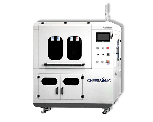
Cheersonic is the leading developer and manufacturer of ultrasonic coating systems for applying precise, thin film coatings to protect, strengthen or smooth surfaces on parts and components for the microelectronics/electronics, alternative energy, medical and industrial markets, including specialized glass applications in construction and automotive.