Innovative approach reveals surprising semiconductor properties
Innovative approach reveals surprising semiconductor properties – Cheersonic
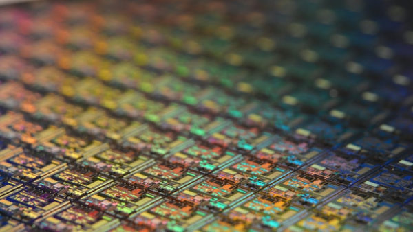
In combination with a new type of thin oxide film, a research team studying the properties of semiconductors has observed a surprising new source of electrical conductivity from oxygen atoms trapped inside.
Scott Chambers, a materials scientist at the Department of Energy’s Pacific Northwest National Laboratory, reported the team’s findings at the 2022 Spring Meeting of the American Physical Society. The findings are described in detail in the journal Physical Review Materials (“Mapping Hidden Space Charge Distributions at Crystalline Metal Oxide/Group IV Semiconductor Interfaces”).
This finding has broad implications for understanding the role of thin oxide films in future semiconductor design and fabrication. Specifically, there are two basic types of semiconductors used in modern electronics—n-type and p-type—depending on the electronic impurities added during crystal growth. Modern electronic devices use n-type and p-type silicon-based materials. But there has been interest in developing other types of semiconductors. Chambers and his team are testing germanium binding to specially crystalline thin films of lanthanum-strontium-zirconium-titanium-oxide (LSZTO).
“We are reporting a powerful tool for probing semiconductor structure and function,” Chambers said. “In this case, hard X-ray photoelectron spectroscopy showed that oxygen atoms (an impurity in germanium) dominate the properties of the material system when germanium is bound to a specific oxide material. This was a big surprise. ”
Using the Diamond Light Source at the Harwell Science and Innovation Campus in Oxfordshire, UK, the team found that they could learn more about the electronic properties of the germanium/LSZTO system than with typical methods.
“The much higher electrical conductivity of germanium basically causes a short circuit when we try to probe this material with conventional techniques,” Chambers said. “So we can learn a little bit about the electronic properties of Ge, which we already know a lot about, but nothing about the properties of the LSZTO thin film or the interface between the LSZTO thin film and germanium – which we suspect could be very interesting, possibly for the technology it works.”
A new role for hard X-rays
The so-called “hard” X-rays produced by the diamond light source can penetrate the material and generate information about what is going on at the atomic level.
“Our results are best explained by the oxygen impurity in germanium, which is a very interesting effect,” Chambers said. “Oxygen atoms near the interface donate electrons to the LSZTO thin film, resulting in holes or absence of electrons in the germanium within a few atomic layers of the interface. In the different samples we prepared, the behavior caused by these special holes is completely beyond The semiconductor properties of n-type and p-type germanium. It was also a big surprise.”
The interface where thin film oxides and base semiconductors come together is where interesting semiconductor properties often arise. The challenge, according to Chambers, is to learn how to control the fascinating and potentially useful electric fields that form at these interfaces by changing the electric field at the surface. Ongoing experiments at PNNL are exploring this possibility.
While the samples used in this study are unlikely to have immediate potential for commercial use, the technical and scientific discoveries made are expected to pay off in the long term, Chambers said. New scientific knowledge will help materials scientists and physicists better understand how to design new semiconductor material systems with useful properties.
Source: nanowerk
Cheersonic is the leading developer and manufacturer of ultrasonic coating systems for applying precise, thin film coatings to protect, strengthen or smooth surfaces on parts and components for the microelectronics/electronics, alternative energy, medical and industrial markets, including specialized glass applications in construction and automotive.