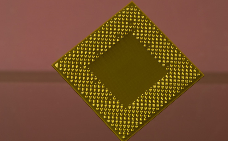
2D Materials For Transistors
2D Materials For Transistors – Electrode Spray – Cheersonic
Two-dimensional materials, the inevitable choice for transistors?
Two-dimensional materials, also known as nanosheets, have attracted much attention in industrial applications because of their excellent electrical and thermal conductivity since graphene was fabricated by artificial methods. Electrons move in two-dimensional materials, because there is no collision caused by movement in another dimension, so under the action of an electric field, they can move faster and improve conductivity. However, graphene itself is a metalloid and lacks the bandgap required for semiconductors, so it cannot be used in the structure of transistors.
However, experts in the material field did not give up, and began to study so-called transition metal disulfides (TMD, such as MoS2, WS2) two-dimensional materials more than ten years ago. TMDs have energy gaps in material properties, so they can be used in The fabrication of transistors, of course, also includes demonstrations of actual transistor components. But we can’t help but ask, are these plans for TMD 2D on-layer transistors expected to be developed by the academic community possible for the industry to use in the next generation of nanodevices?
Silicon-based (Si) transistor components are the core of the semiconductor IC industry. Today’s most advanced ICs contain tens of billions of transistors. In other words, the innovative development of any new transistor must be able to pass the challenge of integration of tens of billions of transistors, including yield and reliability, that is, in the real world, it must face a very difficult entry barrier , otherwise it doesn’t make much sense because it doesn’t solve the problems the industry faces.
A transistor is composed of three basic elements, including material, process and device structure. An IC needs to go through thousands of processes, so the adjustment and improvement of the process can happen at any time. The component structure will also make necessary innovations to solve the problem of characteristics. For example, under the line width of 15 nanometers, the insulating layer was originally above the channel layer, but changed to the upper and lower sides of the channel layer, and finally the channel layer was completely covered by the insulating layer (GAA). The change and innovation of materials is the most difficult, especially in the most critical channel layer of transistors, because it affects the whole body, and this TMD two-dimensional material is exactly the change.
Looking at the core of the transistor over the past two decades, there have been only two changes in materials. One was the introduction of silicon germanium material (SiGe) when entering the 45-nanometer line width, and the other was the introduction of a high dielectric constant (high-K) insulating layer to replace silicon dioxide at 28 nanometers. The purpose of the silicon germanium material is to generate stress near the channel layer, causing the overlapping hole energy bands of the silicon material in the channel to be split, so that the moving speed of the holes can be increased. The introduction of the high dielectric constant insulating layer is to solve the leakage problem that occurs when the insulating layer is too thin. And these two materials have changed. None of the silicon material has moved to the conduction layer.
More than a decade ago, Intel (Intel) used a lot of resources to change the material of the N-type channel to InGaAs and the P-type channel to germanium (Ge) material to improve the conductivity of electrons and holes. . Although this is the best choice in theory, it still cannot solve the defects and reliability problems of crystals in practice, and it falls short. Personally, I cannot assert that TMD two-dimensional materials cannot provide solutions for next-generation transistors, but looking at the historical evolution and objective facts, this chance is very slim.
We are very sure that the government will continue to promote research and development in the semiconductor field to help the industry face the challenges of the next stage. However, the industry has progressed to such a scale that the development of the next generation must carefully select the research and development topics, because the road to be taken must be specialized and refined. In my humble opinion, since fully encapsulated transistors are already a trend, and Moore’s Law will continue to be further extended in the future, 3D stacked transistors are the easiest thing to do. Don’t you see the flash memory (Flash), which has been stacked to 200 layers. In addition, the government can also invest resources in the development of other fields of silicon-based semiconductors, such as 3DIC, MEMS, silicon photonics, sensors, and even compound semiconductors. These investments are the focus of the future of semiconductors.
Source: Content reproduced from digitimes
Cheersonic is the leading developer and manufacturer of ultrasonic coating systems for applying precise, thin film coatings to protect, strengthen or smooth surfaces on parts and components for the microelectronics/electronics, alternative energy, medical and industrial markets, including specialized glass applications in construction and automotive.